what type of a decoder is needed to implement a 64x16 rom?
Read-Only Retention (ROM) is the principal memory unit of whatever computer system along with the Random Access Retentivity (RAM), but dissimilar RAM, in ROM, the binary data is stored permanently . Now, this information to be stored is provided by the designer and is and then stored inside the ROM . Once, it is stored, it remains within the unit, fifty-fifty when power is turned off and on again .
The data is embedded in the ROM, in the course of bits, by a process known equally programming the ROM . Hither, programming is used to refer to the hardware procedure which specifies the bits that are going to be inserted in the hardware configuration of the device . And this is what makes ROM a Programmable Logic Device (PLD) .
Programmable Logic Device
A Programmable Logic Device (PLD) is an IC (Integrated Excursion) with internal logic gates connected through electronic paths that bear similar to fuses . In the original land, all the fuses are intact, merely when we plan these devices, we blow away certain fuses along the paths that must exist removed to achieve a item configuration. And this is what happens in ROM, ROM consists of null but basic logic gates arranged in such a way that they store the specified $.25.
Typically, a PLD can take hundreds to millions of gates interconnected through hundreds to thousands of internal paths . In order to show the internal logic diagram of such a device a special symbology is used, as shown below-
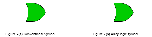
The first image shows the conventional way of representing inputs to a logic gate and the 2nd symbol shows the special mode of showing inputs to a logic gate, called as Array Logic Symbol, where each vertical line represents the input to the logic gate .
Structure of ROM
The block diagram for the ROM is as given below-
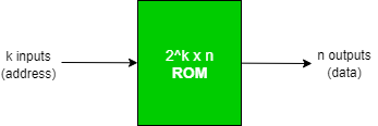
Block Structure
Internal Construction
Nomenclature Of ROM
- Mask ROM – In this type of ROM, the specification of the ROM (its contents and their location), is taken by the manufacturer from the client in tabular grade in a specified format and so makes respective masks for the paths to produce the desired output . This is costly, as the vendor charges special fee from the client for making a particular ROM (recommended, simply if large quantity of the same ROM is required).
Uses – They are used in network operating systems, server operating systems, storing of fonts for light amplification by stimulated emission of radiation printers, sound information in electronic musical instruments .
- PROM – It stands for Programmable Read-Only Retentiveness . Information technology is first prepared as bare memory, and so information technology is programmed to store the information . The difference between PROM and Mask ROM is that PROM is manufactured every bit blank retentiveness and programmed after manufacturing, whereas a Mask ROM is programmed during the manufacturing procedure.
To programme the PROM, a PROM developer or PROM burner is used . The procedure of programming the PROM is called as burning the PROM . Also, the data stored in it cannot be modified, so it is called every bit ane – fourth dimension programmable device.Uses – They accept several unlike applications, including cell phones, video game consoles, RFID tags, medical devices, and other electronics.
- EPROM – It stands for Erasable Programmable Read-Simply Retention . It overcomes the disadvantage of PROM that once programmed, the stock-still pattern is permanent and cannot be contradistinct . If a bit pattern has been established, the PROM becomes unusable, if the flake design has to be changed .
This problem has been overcome by the EPROM, every bit when the EPROM is placed under a special ultraviolet calorie-free for a length of time, the shortwave radiations makes the EPROM return to its initial land, which then can exist programmed accordingly . Over again for erasing the content, PROM programmer or PROM burner is used.
Uses – Before the advent of EEPROMs, some micro-controllers, like some versions of Intel 8048, the Freescale 68HC11 used EPROM to store their program .
- EEPROM – It stands for Electrically Erasable Programmable Read-Only Retention . It is similar to EPROM, except that in this, the EEPROM is returned to its initial state past awarding of an electrical indicate, in identify of ultraviolet light . Thus, it provides the ease of erasing, as this tin can be done, even if the retentivity is positioned in the figurer. Information technology erases or writes ane byte of information at a time .
Uses – Information technology is used for storing the estimator system BIOS.
- Wink ROM – Information technology is an enhanced version of EEPROM .The difference betwixt EEPROM and Flash ROM is that in EEPROM, only 1 byte of information can exist deleted or written at a detail time, whereas, in flash retention, blocks of information (usually 512 bytes) can be deleted or written at a item time . So, Wink ROM is much faster than EEPROM .
Uses – Many modern PCs have their BIOS stored on a wink memory chip, called every bit flash BIOS and they are too used in modems as well.
Programming the Read-But Memory (ROM)
To understand how to program a ROM, consider a 4 x 4 ROM, which ways that it has total of 4 addresses at which data is stored, and each of those addresses has a 4-bit information, which is permanent and must exist given every bit the output, when we access a particular address . The following steps need to be performed to program the ROM –
- Construct a truth table, which would decide the content of each address of the ROM and based upon which a particular ROM will exist programmed.
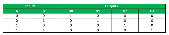
So, the truth table for the specification of the 4 ten iv ROM is described equally below :
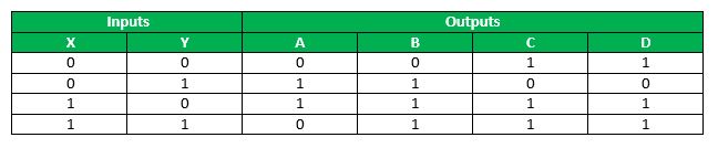
This truth table shows that at location 00, content to be stored is 0011, at location 01, the content should be 1100, and then on, such that whenever a particular address is given as input, the content at that particular address is fetched . Since, with 2 input bits, 4 input combinations are possible and each of these combinations hold a 4-scrap information, so this ROM is a 4 X iv ROM .
- Now, based upon the total no. of addresses in the ROM and the length of their content, decide the decoder as well as the no. of OR gates to be used .
Generally, for a 2 10 n ROM, a k x ii decoder is used, and the total no. of OR gates is equal to the full no. of bits stored at each location in the ROM .
So, in this case, for a 4 x iv ROM, the decoder to be used is a 2 x iv decoder.
The following is a two x 4 decoder –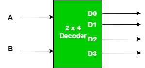
The truth table for a 2 10 4 decoder is as follows –
When both the inputs are 0, then only D
 is 1 and remainder are 0, when input is 01, then, but D
 is high and so on. (Just remember that if the input combination of the decoder resolves to a particular decimal number d, and so at the output side the final which is at position d + 1 from the top volition be 1 and rest will be 0).
Now, since we desire each address to shop iv – $.25 in the four x 4 ROM, then, at that place will be four OR gates, with each of the 4 outputs of the decoder being input to each one of the 4 OR gates, whose output volition be the output of the ROM, as follows –
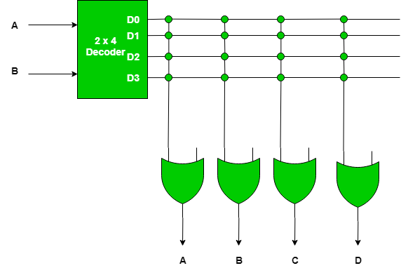
A cross sign in this figure shows connection between the two lines is intact . Now, since there are 4 OR gates and 4 output lines from the decoder, and then at that place are total of xvi intersections, chosen as crosspoint .
- Now, program the intersection between the two lines, equally per the truth table, and so that the output of the ROM ( OR gates ) is in accordance with the truth table .
For programming the crosspoints, initially all the crosspoints are left intact, which ways that information technology is logically equivalent to a airtight switch, but these intact connections tin be blown by the application of a high – voltage pulse into these fuse, which will disconnect the 2 interconnected lines, and in this fashion the output of a ROM can be manipulated .So, to program a ROM, merely look at the truth table specifying the ROM and blow away (if required) a connection . The connections for the 4 ten 4 ROM as per the truth tabular array is as shown below –
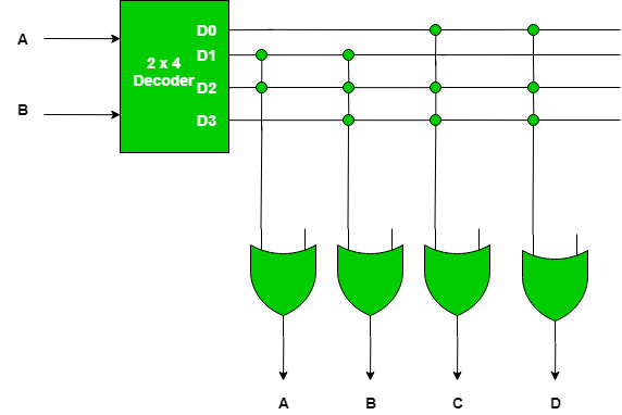
Call up, a cantankerous sign is used to denote that the connection is left intact and if there is no cross this means that at that place is no connection .
In this figure, since, as can be seen from the truth table specifying the ROM, when the input is 00, so, the output is 0011, so equally nosotros know from the truth tabular array of a decoder, that input 00 gives output such that merely D
is 1 and rest are 0, and so to get output 0011 from the OR gates, the connections of D with the first two OR gates has been blown away, to get the outputs as 0, while the last ii OR gates requite the output as 1, which is what is required .Similarly, when the input is 01, then the output should be 1100, and with input 01, in decoder only D
is ane and rest are 0, then to get the desired output the first ii OR gates have their connection intact with D, while last 2 OR gates accept their connectedness diddled away . And for the rest besides the same procedure is followed .
And so, this is how a ROM is programmed and since, the output of these gates volition remain constant everytime, so that is how the information is stored permanently in the ROM, and does not get altered even on switching on and off .
Reference-
- Fundamental of Digital Circuits by A. Anand Kumar
This article is contributed by Mrigendra Singh. If y'all similar GeeksforGeeks and would like to contribute, you can as well write an article using contribute.geeksforgeeks.org or mail your commodity to contribute@geeksforgeeks.org. Encounter your article appearing on the GeeksforGeeks main page and help other Geeks.
Please write comments if you observe anything wrong, or you lot want to share more than information about the topic discussed to a higher place.
Source: https://www.geeksforgeeks.org/classification-and-programming-of-read-only-memory-rom/
0 Response to "what type of a decoder is needed to implement a 64x16 rom?"
Post a Comment